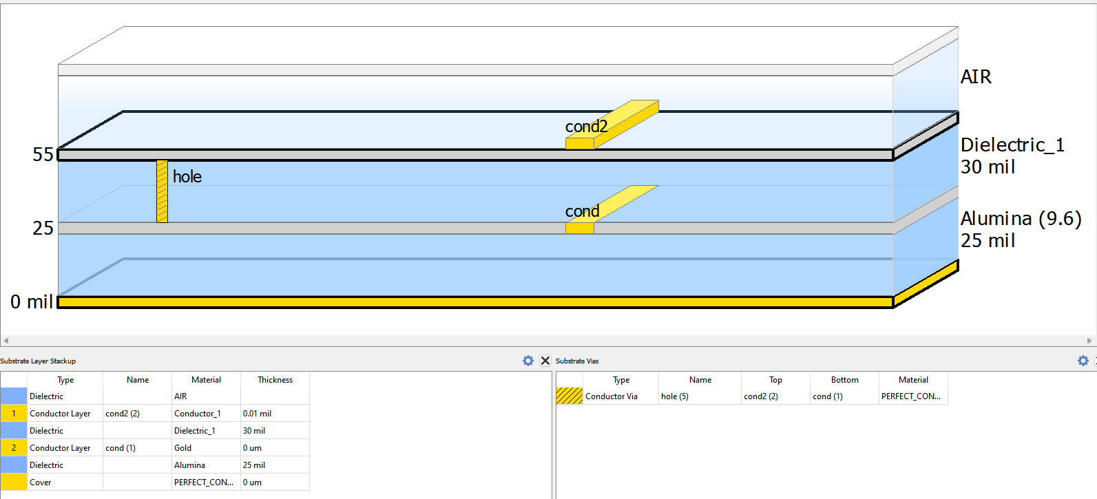
Substrate with Layout
This example demonstrates creating a simple layout with its associated substrate.
# Copyright Keysight Technologies 2024 - 2024
from keysight.ads import de
from keysight.ads import subst as subst
from keysight.ads.de import db_uu
from keysight.ads.de.db import LayerId


def configure_library_tech(library: de.Library) -> None:
    # Configures the library for the example by copying the tech from standard ADS libraries
    library.setup_schematic_tech()
    library.create_layout_tech_std_ads("mil", 10000, True)


def create_layout(library: de.Library) -> db_uu.Design:
    layout = db_uu.create_layout(f"{library.name}:My_Substrate_Example:layout")

    # Add a 300x100 rectangle on the left on layer "cond:drawing"
    cond = LayerId.create_layer_id_from_library(library, "cond", "drawing")
    layout.add_rectangle(cond, (0, 0), (300, 100))

    # Add a 200x100 rectangle overlapping first rectangle on the right on layer "cond2:drawing"
    cond2 = LayerId.create_layer_id_from_library(library, "cond2", "drawing")
    layout.add_rectangle(cond2, (200, 0), (400, 100))

    # Add a radius 30 circle in the overlapping portion of the two rectangles on layer "hole:drawing"
    hole = LayerId.create_layer_id_from_library(library, "hole", "drawing")
    layout.add_circle(hole, (250, 50), 30)

    # Add a pin on the ground net on the left side of the cond layer's rectangle
    gnd_net = layout.find_or_add_net("gnd!")
    term_1 = layout.add_term(gnd_net, "P1")
    pin1_pinfig = layout.add_dot(cond, (0, 50))
    layout.add_pin(term_1, pin1_pinfig, angle=180.0)

    # Add a pin on the ground net on the right side of the cond2 layer's rectangle
    term_2 = layout.add_term(gnd_net, "P2")
    pin2_pinfig = layout.add_dot(cond2, (400, 50))
    layout.add_pin(term_2, pin2_pinfig)

    # Save changes to the layout file
    layout.save_design()

    return layout


def create_substrate(library: de.Library) -> subst.Substrate:
    # Create a new substrate using "25milAlumina" as a starting point
    substrate = subst.create_substrate_from_template(library, "example_substrate", "25milAlumina")

    # Configure the cond layer to be a Gold sheet
    cond = substrate.layers[0]
    cond.layer_number = LayerId.create_layer_id_from_library(library, "cond", "drawing").layer
    cond.sheet = True
    cond.material_name = "Gold"

    # Inserts a new material at the given index with an interface directly above it
    substrate.insert_material_and_interface_above(substrate.top_material_index)
    # Find the newly created material and set its properties
    dielectric = substrate.get_material_above(cond.interface)
    # Note this material will need to be defined manually in the library's technology
    dielectric.material_name = "Dielectric_1"
    dielectric.thickness = 30

    # Insert the cond2 layer
    cond2_interface = substrate.get_interface_above(dielectric)
    cond2 = substrate.insert_layer(cond2_interface, de.ProcessRole.CONDUCTOR)
    cond2.layer_number = LayerId.create_layer_id_from_library(library, "cond2", "drawing").layer
    # Set cond2 to intrude above the interface
    cond2.expand = False
    cond2.sheet = False
    cond2.is_above = True
    # Note this material will need to be defined manually in the library's technology
    cond2.material_name = "Conductor_1"

    # Create the via between the cond and cond2 layers
    via = substrate.insert_conductor_via(cond.interface, cond2.interface)
    # Set the via layer to "hole:drawing" to match the layout
    via.layer_number = LayerId.create_layer_id_from_library(library, "hole", "drawing").layer
    via.material_name = "PERFECT_CONDUCTOR"

    # Save all our changes to the substrate file
    substrate.save_substrate()
    return substrate
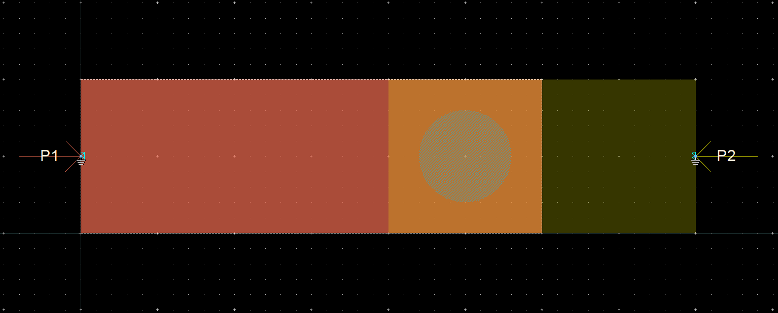
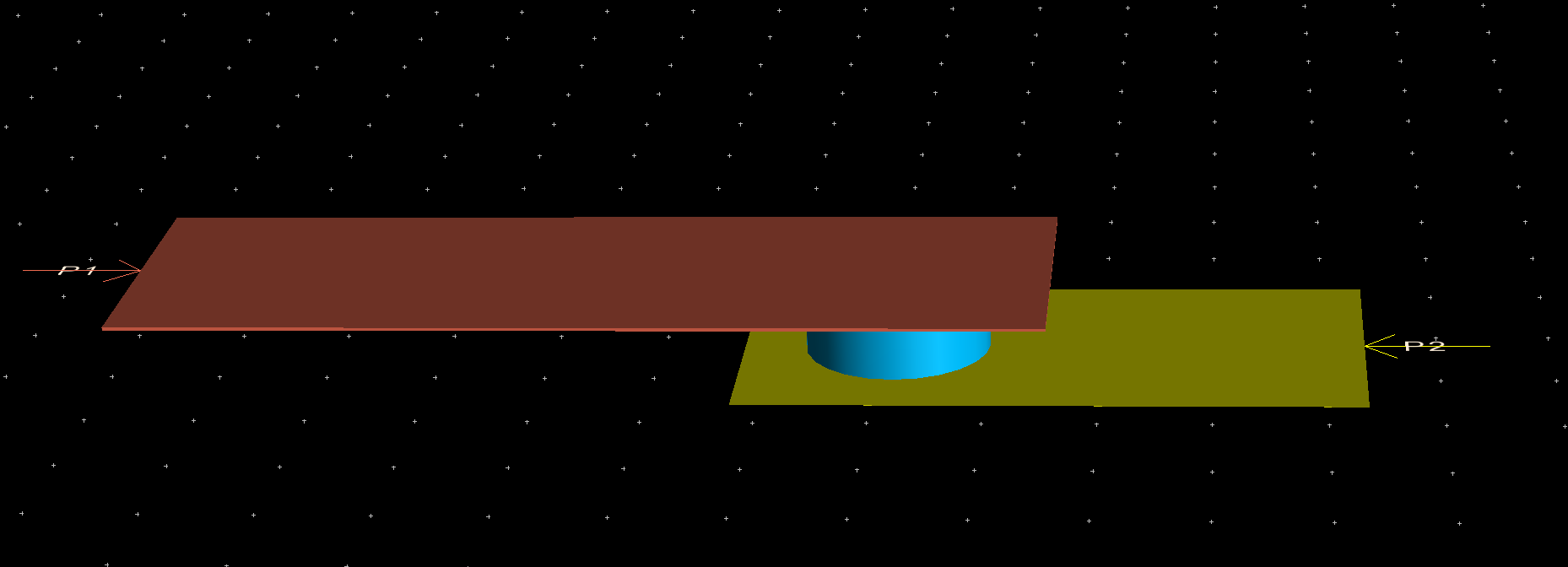
The layout includes two metal conductors on differing layers connected by a via:
The substrate defines the materials and thicknesses of the design created in the layout: